As someone who enjoys tinkering with electronics as a hobby, I’ve always been intrigued by the idea that one may create a Printed Circuit Board (PCB) that looks practically identical to a commercially produced one.
As time passes and the availability of through-hole packages (for modern devices) decreases, my desire to produce my PCBs at home rather than using the suitable old wire-wrap prototyping method grows. If SMT technology is permissible, there is a far more comprehensive range of devices to choose from when conceptualizing a new design. That’s a terrific incentive to study how to fabricate SMT PCBs on time.
There has been a lot of success with the technique I’m about to describe, and the outcomes are stunning. Observing regulations is crucial. It’s the kind of creation that, once finished, makes you feel fantastic.
Once again, according to the guidelines will ensure a smooth procedure. At first glance, this may appear to be a complicated procedure; nevertheless, it is relatively simple.
Critical processes in manufacturing:
Step 1: Use a laser printer to create a mirror image of your circuit, which you will then transfer to the toner transfer paper.
Copper-over-glass epoxy laminate should be cut, sanded, and cleaned.
Put your finished artwork in the oven and bake it.
To number four, immerse your board in etching chemicals.
5. Sand any leftovers and rinse with water.
6. Display your board for everybody to see.
Seven, join the parts with solder.
A few remarks:
When following these instructions, be sure to prioritize safety.
When handling the etching chemical, latex gloves are strongly suggested.
There are various ways to become hurt, from cuts and burns to ruined garments and inhaled chemicals while working on a production. Take care.
What are we waiting for?
Like any other modern device, your PCB would begin life in some design program on your computer. The scope of this guide does not include the decision of which design program to use for this work. The only thing I demand is the ability to print a mirror image of the design. It’s difficult to explain why replicating the plan is crucial, but the photos at the link below should help.
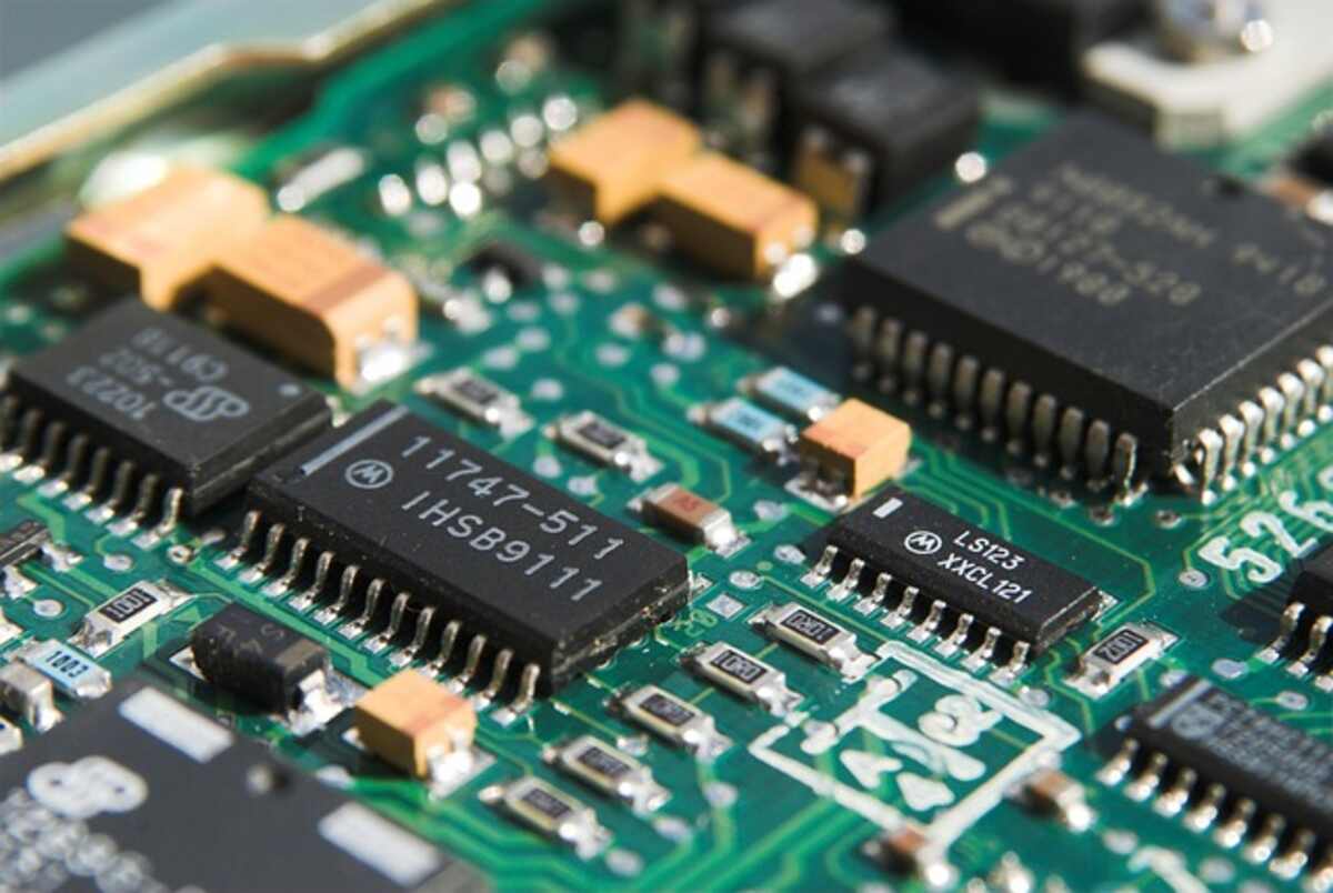
Eliminating the need to drill holes through the board for SMT devices is a significant benefit of an SMT-based PCB for DIY manufacturing. Wow, that’s fantastic. This isn’t always possible, though. Drilling holes is only necessary for a select few situations. As an illustration, not many connectors call for pre-drilled holes. In addition to drilling, solder bridging traces that cannot be routed in copper would necessitate drilling. Whatever the case, SMT technology drastically reduces the number of drilled holes while minimizing the size of the board.
My goal in bringing up the SMT benefit was to get you to think about how few drills you want your circuit to require and how you should strive to avoid complex designs altogether. When possible, I like to split up extensive courses over multiple boards. This division of the board is happening for two main reasons. To begin, a more straightforward layout is possible using a smaller circuit. Second, in the future, larger designs may be able to incorporate more miniature courses as fundamental, general-purpose building blocks. Consider a multi-function operational amplifier circuit board. A simple OPAMP device with some surrounding resistors and solder pads for connecting wires to the outside world could be on such a board. It serves as a solid foundation for a wide range of endeavors. Once your layout design is ready for production, you may print a mirror image at a 1:1 scale using a laser printer and some special glossy paper (Toner Transfer paper would be excellent).
Let’s chop up that last sentence into manageable chunks.
The completed design should resemble a schematic of the circuit board regarding the placement of traces. Because of how the image will be used in the next step, it must be flipped horizontally. For example, “some paper used by inkjet printers for photo printing” falls under “glossy paper,” a generic phrase for a more nebulous description. In case you were unaware, there is a difference between picture sheets. It could be time-consuming to track the ideal paper for this task. The first piece of paper I tried to use could not be removed from the PCB, so I had to toss it. The following article I came across was a winner. It’s simple to remove, and all left on the bare copper is a clear imprint of the traces. This peeling problem is something I’ll get to in a bit. Remember that it may take a few different picture papers before discovering the perfect one. Don’t just give up on it. Fortunately, this problem can be solved by using Toner Transfer Papers.
If you want your printed circuit board to exactly match the physical size of your components and traces, you should use a 1:1 scale setting in your software. Finally, laser printing is the only option. Since the black substance (laser “ink”) used for laser printing is a polymer rather than ink, it does not absorb into the paper as traditional ink does. The printer’s internal heat causes the toner to melt and adhere to the glossy paper. When heated, the toner on the paper’s surface will melt and transfer to everything it comes into contact with. Is it starting to click for you?
Now that we have a printed copy of our PCB, we can trim the paper to the board’s exact dimensions while leaving a little margin of paper around the outside. We’ll need this scrap beyond the board’s borders to handle when it’s time to remove the backing.
The fun part comes when we make something with our own two hands!
First, a glass epoxy substrate (FR4 laminate) is laminated with a thin copper layer. Most laminates can be obtained in the same stores as electrical parts. Two varieties of laminates are available to the average homeowner. Two types: one- and two-sided. Typical thickness is 1-2 mm. “single-sided” refers to laminates with copper on only one side. Copper is present on both sides of the laminate, hence the term “dual.” Single-sided laminate is adequate since only one side of the PCB is being used in this study. Since any excess copper may be etched away during fabrication, single-sided circuits can be constructed from single- or double-sided laminates.
The process of cutting the laminate to the size of the circuit happens in two stages. Using a sharp knife and a ruler, you must first mark the height of your course across the laminate. The less complicated it will depend on how deep you characterize. Once you’ve drawn the line, you can align a ruler above the laminate with a table’s edge. Applying force to the laminate should cause it to crack at the line of demarcation, revealing a clean, straight edge. Now mark and cut the circuit to the exact width indicated.
Related Posts
We should get the laminate ready for the toner transfer process now that it has been trimmed to size. Copper should be sanded uniformly using the finest sandpaper (wet paper) until it is clean and bright, leaving minute scratches on the surface. These minute abrasions are ideal anchor points for the toner’s adhesion to the copper.
Soap and water should be used to clean the laminate after sanding the copper. Dishwashing liquid is the finest option. This washing attempts to eradicate grease residue (including fingerprint grease). Toner would not adhere to the copper properly if oil were still present. After washing the copper, please don’t touch it again unless you want greasy fingerprints. The final step is to dry the laminate using a paper towel.
Do you recall the glossy paper with the reverse picture printed on it? Position it so the copper is up, and the toner is down, with the copper facing up. There should be no slant between the paper and the copper. Keep the paper and laminate still and secure them with tape along two edges. Verify that the circuit is set up as desired, and
relax; the exciting part is just around the corner.
It’s time to put your circuit in the oven. Few advocate pressing the paper with a hot iron until it adheres to the copper. Ironing, in my experience, is not consistently successful at transferring toner. It can be effective, but there are also times when it fails. I think I finally figured out a suitable method. You’ll need a pressing mechanism to keep the glossy paper pressed onto the copper while the oven preheats and bakes. I employ two square sheets of aluminum with holes drilled into the corners. The plates with the circuit in the middle are bolted together. The course needs to be wrapped in several layers of paper for protection. Padding is essential to prevent uneven pressure distribution over the laminate and subsequent improper circuit transmission. The laminate and shiny paper should be pressed with a lot of force, so ensure the bolts and nuts are secured tight.
The press needs to be baked in an oven warmed to 150 degrees Celsius for 30 minutes. The press device’s mass will determine the baking time. It takes longer for the press to heat up to the point where the heat can be transferred to the paper padding and the circuit within a heavier press. It’s best practice to wait until the oven is cold enough to touch before opening the door once baking is complete. Now is the time to undo the screws and read the schematics hidden beneath the stacks of paper.
The shiny paper should be firmly adhered to the copper if the procedure is successful. Now, grab the report by an edge and slowly pull it away from the copper. Removing the paper from the copper will reveal a beautiful print if you’re lucky. You may have trouble removing the form without damaging the printed traces on the copper if it is not friendly. Inadequate pressure distribution can cause some toner to fail to adhere to the copper, rendering the laminate worthless for further processing (though it can always be sanded down and started over). If everything went according to plan, you should now be holding in your hands a laminate upon which your circuit has been printed as if it were a piece of paper fresh from a laser printer.
If any through-hole packages or bridging wires need to be drilled before etching can begin, you can do it now. Since the surrounding copper provides greater mechanical strength to the circular pads around the drilled holes, preparing before etching begins is recommended. After engraving the board, drilling may occasionally rip off these pads. As an additional benefit, the drilled hole’s borders would be free of copper strands thanks to the etching process that follows drilling.
Excess copper should now be removed where there are no traces (no toner). The toner is a barrier, keeping the etching fluid away from our paths. Ferric chloride, often known as etching material, is available for purchase as small gravel or powder.
Warm water (the kind you’d use to wash your hands on a chilly day) and Ferric-Chloride make up the etching solution. Quantity to quality is not an issue. Too little Ferric-Chloride would slow down the etching process. When used in excess, the fluid becomes black and muddy. Like brewing a cup of coffee, I employ ratios. Fill your container with water, then add a small amount of Ferric-Chloride to the bottom. Metal is not recommended for the etching container’s construction.
The circuit must be continuously lowered into and retrieved from the etching fluid. This allows the fluid to reach into the deeper copper layers by removing any etched copper traces from the surface. I have what looks like a small fishing pole with a line attached to a tiny hole I drilled into the lamination. It may take a few minutes of etching before you notice any results after you’ve started the process. At first, the exposed copper disappears from vast areas. The voids between traces will become apparent in only a few more minutes. The board will be completed in thirty minutes or so.
The etching process can be stopped by washing the board under running water as soon as it reaches the desired appearance. Wash the circuit (and the storage container) with care. The black fluid will discolor anything it touches.
The final step can be completed after the circuit has been cleaned. The black toner must be scrubbed away with the finest sandpaper (wet paper) to reveal the copper. Alternatively, you might wash it with a few drops of acetone to remove the black toner. Soldering can begin once all copper on the board has been exposed.
It ends here. You’re holding your first PCB that wasn’t mass-produced. It’s time to show off your accomplishments now. Just connect the wires and flip the switch to finish the circuit…
Viewing the images at the provided website is highly advised.
Check out the images that accompany this piece:
A Step-by-Step Guide to Making Printed Circuit Boards (PCBs) from the comfort of your home with a laser printer or Toner Transfer Technique.
Read also: How to Avoid Falling Victim to Different Ransomware Schemes